

Optical filters—key in optical systems for selective light transmission/reflection—rely heavily on substrate fabrication quality, especially chamfering and edge processing. These processes (controlled edge beveling/finishing) minimize stress, prevent chipping, and boost mechanical and optical performance.
But they pose major technical challenges, which impact subsequent thin-film coating and final filter reliability. This document analyzes these key challenges, their effects on coating integrity, and offers practical, standard-compliant solutions (ISO 10110, MIL-PRF-13830) for production lines.
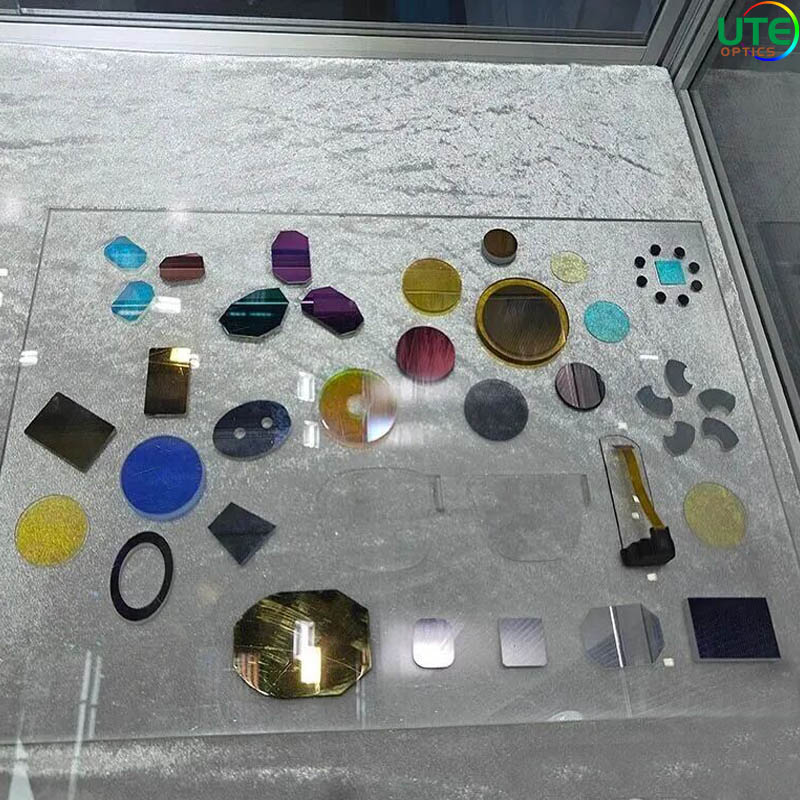
I. Analysis of Challenges in Chamfering and Edge Processing
Filter substrates are commonly fabricated from brittle, high-hardness materials such as optical glass, crystalline substances, or advanced ceramics, all of which demand exceptional precision during machining. The principal challenges include:
1. Chipping and Microcrack Formation Due to Material Brittleness
Brittle materials are susceptible to fracture during mechanical processing, particularly at peripheral regions. The application of cutting forces or grinding pressure during chamfering may induce microcracks or localized chipping—forms of edge damage—that can propagate during downstream processes, compromising structural integrity.
Key Challenges: Control of chipping dimensions, detection and mitigation of subsurface microcracks. For instance, in high-strength glasses such as fused silica or BK7, the likelihood of chipping increases markedly when chamfer angles fall below 30°.
2. High Precision and Batch Consistency Requirements
Chamfer geometry—including width, angle, and contour—must conform strictly to design specifications, typically within dimensional tolerances of ±0.1 mm and angular tolerances of ±1°. Achieving uniformity across large production batches remains a significant challenge.
Key Challenges: Equipment precision, tool wear management, and variability in operator technique. Inconsistent edge profiles may result in assembly misalignment or contribute to optical aberrations.
3. Surface Quality and Smoothness
Edges must attain optical-grade surface finish, with a roughness average (Ra) ≤ 0.1 μm, to minimize stress concentration and suppress stray light generation. Conventional machining methods often leave behind tool marks, burrs, or subsurface damage.
Key Challenges: Difficulty in achieving fine surface finishes, especially on small-diameter or complex-shaped substrates. Poor edge smoothness contributes to increased light scattering, thereby degrading filter contrast and signal-to-noise ratio.
4. Thermal and Mechanical Stress Generation
Processing-induced thermal stresses (e.g., from frictional heating) and mechanical loads can lead to substrate deformation or residual stress accumulation, adversely affecting surface flatness and wavefront fidelity.
Key Challenges: Effective thermal management through cooling strategies and optimization of process parameters. For example, excessive localized heat during high-speed grinding may initiate microcrystallization in certain glass types.
5. Cleaning and Contamination Control
Particulate debris and residual coolants generated during edge processing can adhere to the substrate surface, impairing the adhesion and purity of subsequently deposited coatings.
Key Challenges: Development of robust cleaning protocols, particularly for porous or pre-coated substrates, to ensure complete removal of contaminants without surface damage.
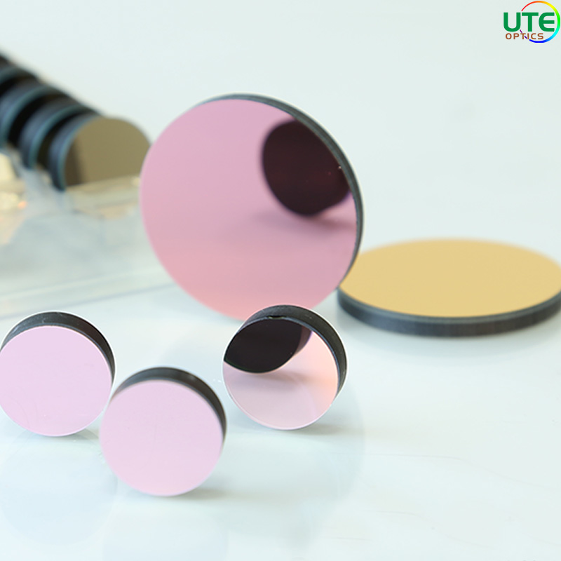
II. Impact of Edge Quality on Thin-Film Coating Performance
The integrity of chamfering and edge finishing directly influences the uniformity, adhesion, and long-term durability of optical coatings, thereby determining overall filter performance. Major effects include:
1. Reduced Coating Uniformity
Edge defects such as chipping or burrs disrupt vapor flux distribution during physical vapor deposition (PVD) or chemical vapor deposition (CVD), leading to non-uniform film thickness at critical boundary zones.
Practical Consequences: Spectral shifts in center wavelength, altered bandwidth, and reduced peak transmission. In bandpass filters, edge-related thickness variations may manifest as passband ripple or elevated side lobes.
2. Weakened Coating Adhesion
Stress concentration at sharp edges or within microcracked regions promotes delamination or crack initiation in the coating layer. Under environmental stressors such as thermal cycling or mechanical vibration, this accelerates coating failure.
Practical Consequences: Premature onset of the "edge effect"—progressive peeling of the coating starting from the periphery—diminishing device reliability and environmental resilience.
3. Increased Light Scattering and Stray Light
Rough or irregular edges act as scattering centers, redirecting incident light into unintended paths and elevating system-level stray light.
Practical Consequences: Degraded image contrast and reduced signal-to-noise ratio; particularly detrimental in high-precision imaging systems, where it may cause image blurring or elevated background noise.
4. Stress-Induced Performance Degradation
Residual stresses from substrate processing combine with intrinsic stresses in the deposited film, potentially inducing substrate bending or cohesive film cracking, thereby altering the effective optical path length.
Practical Consequences: Drift in spectral characteristics over time and compromised long-term stability of filter performance.
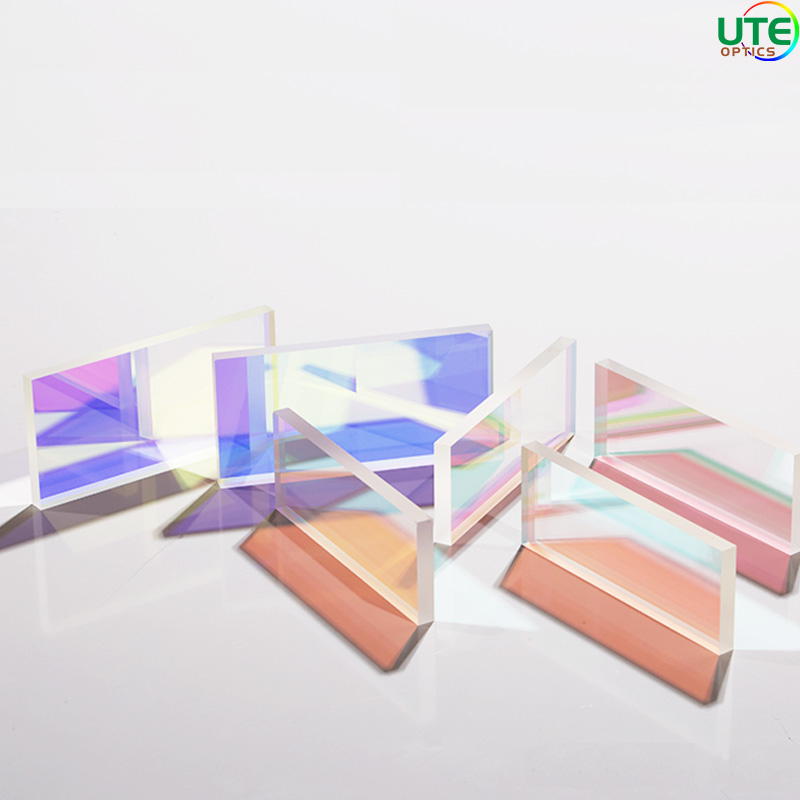
III. Recommended Mitigation Strategies
To address the aforementioned challenges and their implications for coating performance, the following evidence-based, industry-compatible solutions are proposed. These approaches emphasize process refinement, quality assurance, and adherence to international optical manufacturing standards, without requiring extensive capital investment.
1. Optimization of Chamfering Processes
Utilize high-precision CNC-controlled chamfering machines equipped with diamond or cubic boron nitride (CBN) tools to ensure geometric consistency and dimensional accuracy. Process parameters should be tightly regulated: feed rates ≤ 0.1 mm/rev and spindle speeds ≥ 5000 rpm to minimize dynamic loading. Implement a two-stage approach: coarse grinding with #400-grade diamond wheels for initial shaping, followed by fine grinding using #2000-grade abrasives to refine edge finish and reduce subsurface damage. Employ continuous flow of water-based or specialized optical coolants (flow rate ≥ 5 L/min) with filtration systems to manage heat and remove particulates effectively.
2. Post-Processing Edge Finishing Techniques
Chemical polishing: Apply hydrofluoric acid (HF)-based etchants (e.g., HF:NH₄F = 1:5) for brief durations (30–60 seconds) to dissolve microcracks and achieve smooth edges on glass substrates, while avoiding over-etching.
Flame polishing: Use hydrogen-oxygen flames for rapid surface melting and smoothing of compatible glass types; requires precise temperature control to prevent warping.
Mechanical polishing: Finalize edges using soft polishing media (e.g., polyurethane or felt wheels) with cerium oxide or silica-based slurries under low pressure (<0.1 MPa) for 1–2 minutes to achieve Ra ≤ 0.1 μm.
3. Quality Assurance and Inspection Protocols
Integrate automated optical inspection systems (e.g., CCD cameras or laser profilers) for real-time measurement of chamfer dimensions and defect detection. Set acceptable thresholds for chipping size at ≤50 μm using image analysis software. Conduct residual stress evaluation via polariscopes or digital speckle interferometry, ensuring edge stress levels remain below material yield limits (e.g., <10 MPa for optical glass). Implement ultrasonic cleaning with deionized water and neutral detergents, followed by nitrogen blow-drying, to eliminate particulate and chemical residues.
4. Pre-Coating Edge Treatments
Edge passivation: Apply mild abrasive treatments (e.g., alumina micro-powder, particle size ≤10 μm, at 0.2–0.5 bar pressure) to enhance coating adhesion.
Coating design compensation: Incorporate graded or transitional layers (e.g., SiO₂) near the edge zone to mitigate stress discontinuities and reduce edge field intensity in multilayer stacks.
5. Standardization and Workforce Development
Provide regular training programs for operators focusing on parameter control, defect recognition, and procedural compliance. Establish documented standard operating procedures (SOPs) encompassing machining settings, inspection criteria, and equipment maintenance schedules to ensure cross-line consistency and traceability.
In conclusion, chamfering and edge processing represent pivotal stages in optical filter manufacturing, where substrate quality directly governs coating performance and product longevity. By systematically addressing critical challenges—including chipping, dimensional accuracy, surface finish, and stress management—and understanding their cascading effects on thin-film deposition, manufacturers can implement targeted improvements in process control and quality assurance. The strategies outlined herein are consistent with international optical standards and are readily adaptable to existing production environments, enabling enhanced filter performance and reduced yield loss. Looking ahead, continued advancements in automation, in-process monitoring, and novel materials will further drive the evolution of edge processing toward higher precision, efficiency, and reproducibility.