

In high-end fields like optical imaging, laser systems, and spectral analysis, optical filters act as core components for light path control. Their surface form accuracy and surface quality directly determine the ultimate performance of the entire system. However, at every stage of their production—from substrate cutting, grinding, and polishing to coating and cleaning—lurk "invisible killers" that can render finished products non-functional: surface and edge defects. These defects, measuring just micrometers or even nanometers, not only reflect manufacturing craftsmanship but also serve as decisive factors for optical performance.

I. Scientific Classification and Formation Mechanisms of Defects
In professional terminology, filter processing defects are typically categorized by their location and nature into the following types:
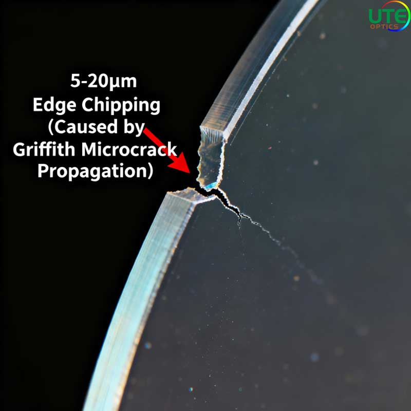
1.1 Edge Defects: Chipping
Edge chipping refers to microscopic or macroscopic fractures, peeling, or notches that occur at the edge of a filter. It is a classic issue in brittle material processing.
Formation Mechanisms:
Brittle material fracture: Optical glass is a typical brittle material, and its fracture behavior follows Griffith’s Microcrack Theory. Pre-existing microcracks within the material experience stress concentration at their tips when subjected to external tensile stress. Once the stress exceeds the critical threshold, the cracks expand unstably, leading to brittle fracture.
Processing-induced stress concentration: During mechanical processes such as diamond wheel cutting and edge grinding, cutting forces are highly concentrated at the contact area between the tool and the material. Improper selection of processing parameters (e.g., feed rate, cutting depth, grit size, and binders) or ineffective coolant (failing to remove cutting heat and debris) can generate local stress sufficient to propagate cracks—resulting in chipping.
Fixture and clamping stress: Unreasonable fixture design (e.g., overly small contact area, improper V-block angle) or excessive clamping force creates intense contact stress at clamping points, directly crushing the filter’s edges.
1.2 Surface Defects: Scratches and Scuffs
Professional standards (e.g., MIL-PRF-13830B) generally refer to surface imperfections as "scratches," but they can be further classified by morphology and cause:
Scratches
Linear or groove-like damage on the optical surface, created when one or a few hard particles slide under pressure. They typically have a small width-to-depth ratio.
Formation Mechanisms:
Particle contamination: This is the primary cause. Abrasive particles (e.g., diamond powder, cerium oxide) used in grinding and polishing—if not fully removed during subsequent cleaning—or environmental hard particles (e.g., silica dust from air, personnel, or equipment) become "microscopic blades" when trapped between the workpiece and polishing pads, wipes, or transfer rails.
Three-body abrasion: In the scenarios above, hard particles act as independent "third bodies," rolling and sliding freely between two contact surfaces to cause scratches.
Scuffs
Wider, shallower surface damage—sometimes appearing as a network or dense pattern of shallow marks.
Formation Mechanisms:
Two-body abrasion: Direct sliding friction between the filter’s optical surface and equipment carriers, other workpieces, or substandard soft tools (e.g., gloves with impurities, lint-free cloths).
Soft particle aggregation: Even soft materials, if covered in large quantities of tiny particles, can cause extensive shallow scuffs when under pressure.
1.3 Structural Defects: Cracks
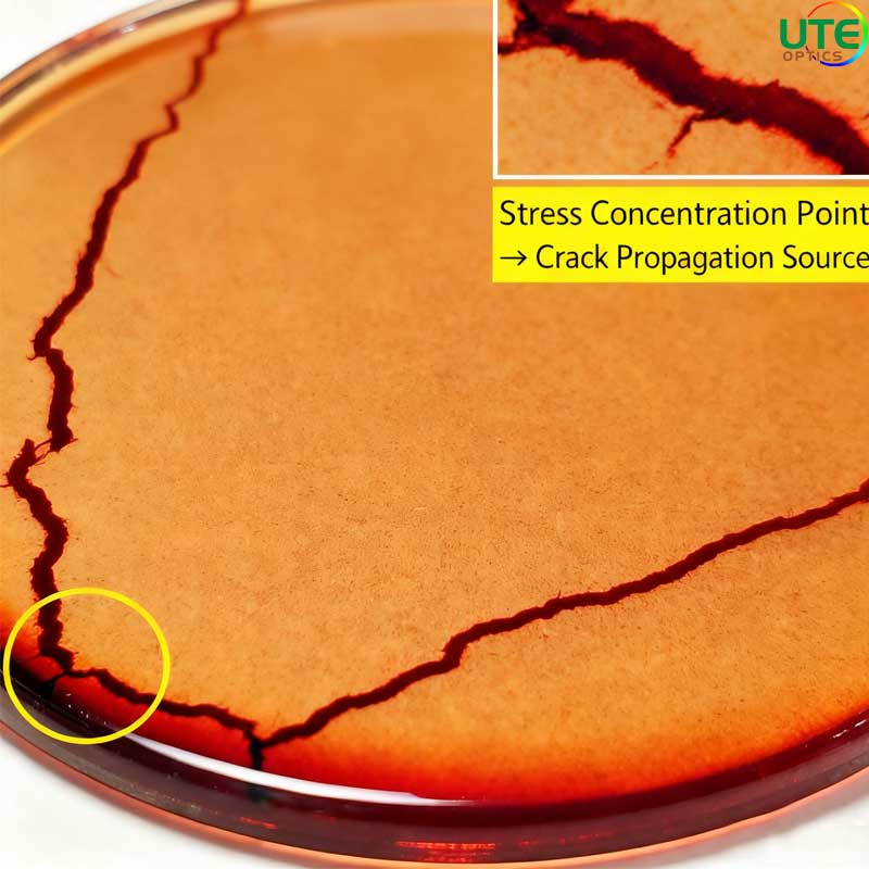
Cracks are continuous fissures that penetrate the surface or extend inward from edges, compromising the material’s integrity.
Formation Mechanisms:
Macro-mechanical impact: Severe impacts during handling, dropping, or assembly can directly create cracks.
Thermal stress cracking:
Film-substrate mismatch: During coating, differences in the coefficient of thermal expansion (CTE) between the substrate and film materials (e.g., Ta₂O₅, SiO₂) generate significant thermal stress at the film-substrate interface as the component cools from the high-temperature coating process. If this stress exceeds the film-substrate adhesion or material strength, cracks form—even leading to film peeling in severe cases.
Rapid temperature fluctuations: Sudden temperature changes during cleaning or processing also create gradient thermal stress within brittle substrates.
Stress concentration effect: A critical causal relationship exists: the base of any "chip" or "deep scratch" is a natural, sharp stress concentration point. Subsequent processing (e.g., polishing pressure, coating thermal stress) or in-service vibrations/thermal cycling causes stress to accumulate here, triggering microcrack initiation and propagation into macroscopic cracks.
II. End-to-End Control: Eliminating Defects with a Precision Quality System
To eliminate defects, a comprehensive precision quality engineering system must be established—spanning design, processing, environment, and operation.
2.1 Process Optimization
For Edge Chipping:
Laser processing: Use ultrafast pulsed lasers for cutting and drilling. Their "cold processing" characteristic minimizes mechanical stress, enabling chip-free manufacturing.
Precision edge grinding: Employ high-rigidity CNC edge grinders with a "micro-cutting depth, slow feed rate, full cooling" process, paired with natural diamond grinding wheels. Optimize the processing path to ensure the final cutting force is directed toward the material’s interior.
Chemical Mechanical Polishing (CMP): Apply CMP to filter edges. This combines chemical etching and mechanical grinding to smoothly remove damaged layers.
For Scratches/Scuffs:
Cleanliness control: Conduct all post-polishing processes in high-grade cleanrooms (e.g., ISO Class 5 / Class 100). Physically isolate areas using different grit abrasives to prevent cross-contamination.
Tooling management: Use inert, soft materials (e.g., PEEK, Teflon) for all fixtures and nozzles that contact workpieces. Perform regular ultrasonic cleaning.
Process automation: Integrate robotic arms and automatic transfer systems to minimize contact risks from human intervention.
2.2 Operational Protocols
Mandatory training: Operators must complete rigorous aseptic operation training, including:
Proper use of nitrile gloves;
Handling workpieces with vacuum tweezers or non-contact tools;
Cleaning with high-purity solvents (e.g., electronic-grade ethanol) and dedicated lint-free paper using a "single-directional wipe" method (wiping once from the center to the edge).
2.3 Process Monitoring & Materials Science
In-line inspection: Install automated machine vision inspection systems after key processes to conduct 100% in-line screening for edge chipping and surface scratches.
Material selection: Within optical design constraints, prioritize optical glass grades with higher fracture toughness and Knoop hardness to enhance inherent damage resistance.
Design optimization: Clearly specify and appropriately enlarge protective chamfer dimensions in drawings to eliminate sharp edges at the design stage.
III. Optical Impacts of Defects: From Theoretical Perfection to Practical Degradation
These microscopic defects exert comprehensive, even catastrophic, impacts on optical performance.
3.1 Deteriorated Imaging Quality
Stray light and reduced contrast: Any scratch, scuff, or chip disrupts the filter’s perfect mirror-like surface, turning it into a light-scattering center. During imaging, this scattered light reaches the image plane unexpectedly, creating uniform "background noise" (haze) that severely reduces contrast. In systems requiring weak target detection (e.g., astronomical telescopes, dark-field microscopes), target signals may be completely drowned out by noise.
Wavefront distortion: Deep scratches and cracks act as physical grooves or fissures, altering the optical path of passing light and introducing wavefront aberrations. This degrades the system’s point spread function (PSF) and modulation transfer function (MTF), directly manifesting as reduced imaging resolution and blurred images.
3.2 Laser System Performance & Reliability Risks
Plummeting laser damage threshold (LDT): For high-energy laser systems, surface and edge defects are the weakest links. Defects significantly enhance laser energy absorption (linear absorption) or trigger nonlinear absorption effects, causing rapid local temperature rises. This leads to melting or ablation of the film or substrate—typically initiating damage at defect sites at power levels far below the LDT of a flawless component. A barely detectable edge chip can serve as the "trigger" for total laser component failure.
3.3 Long-Term Reliability Hazards
Crack propagation: Per fatigue fracture mechanics principles, repeated environmental vibrations and thermal cycling stress drive the gradual expansion of initial microcracks and stress concentrations at chip sites. This can eventually cause unexpected component fracture during service, resulting in catastrophic system failure.
Surface and edge defects in filter manufacturing are by no means trivial "cosmetic issues"—they are core indicators that reflect the precision of manufacturing systems and directly define the performance limits of optical systems. Their prevention and control is a systematic engineering effort encompassing materials science, mechanics, thermodynamics, chemistry, and precision engineering. The pursuit of "zero tolerance" for defects remains the enduring driving force behind advancing cutting-edge optical manufacturing to the nanoscale and supporting the development of next-generation high-end technological equipment.
If needed, I can further refine the English version by adjusting the tone to better align with your independent site’s brand voice (e.g., more technical for engineers or more accessible for procurement teams). Would you like this targeted optimization?